|
Xing WuCareer: Organization: East China Normal University Discipline: |
|
|
|
10 Visits |
Related to the teacher |
About
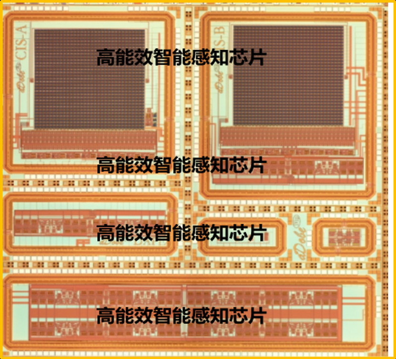
EducationWorkExperienceResumeDr. Xing Wu received her bachelor’s degree in Electronic Engineering from Xi’an Jiaotong University (XJTU) China in 2008 and her PhD degree from Nanyang Technological University (NTU) Singapore in 2012. Then, she worked at the Singapore University of Design and Technology (SUTD) and Southeast University (SEU). She is currently a full professor at East China Normal University (ECNU) China.She has published 136 SCI journal papers including Science, Nat. Nano. Nat. Commun., Adv. Mater., and IEEE TED with more than 5000 citation. She holds 50 patents. Other AppointmentsResearch Fieldssemiconductor materials, semiconductor devices, MEMS, TEM Enrollment and TrainingCourseScientificAcademic AchievementsSensors: F. Liang, C. H. Cai, K. Zhang, L.Zhang, J. Li, H.B. Bi, P. S. Wu, H. Zhu, C. L. Wang, H. Wang, Z. Dong, C. Luo, Z. W. Luo, C. Shan, W. Hu*, and X. Wu*, “Infrared gesture recognition system based on near-sensor computing”, IEEE Ele. Dev. Lett., in publication. F. Liang, C. Wang, C. Luo, Y. Xia, Y. Wang, M. Xu, H. Wang, T. Wang, Y. Zhu, P. Wu, J. Ye, G. Mu, H. Zhu, and X. Wu*, “Ferromagnetic CoSe broadband photodetector at room temperature”, Nanotech., 31, 374002, (2020).
F. Wu, Q. Li, P. Wang*, H. Xia, Z. Wang, Y. Wang, M. Luo, L. Chen, F. S. Chen, J. S. Miao, X. S. Chen, W. Lu, C. X. Shan, A. L. Pan, X. Wu*, W. C. Ren, D. Jariwala, and W. Hu*, “High efficiency and fast van der Waals hetero-photodiodes with a unilateral depletion region”, Nat. Commun., 10:4663 (2019).
T. Fan, Z. Liu, J. Li, Z. Luo, J. Li, X. Tian, C. Wang, H. C. Bi, X. M. Li*, F. Qiao*, X. Wu*, “Analog sensing and computing system with low-power consumption for gesture recognition”, Advanced Intelligent Systems, 2000184,(2020). 入选人工智能类hot topic
X. Tian, Z. Liu, Z. Luo, X. Wu*, F. Qiao*, X. Wang, G. Li, J. Wu, J. Zhang, Z. Liu, and J. H. Chu, “Dual-mode sensor and actuator to learn human hand tracking and grasping”, IEEE Trans. Elec. Dev., 6, 12, (2019). Z. W. Luo , X. T. Hu , X. Y. Tian , C. Luo , H. J. Xu , Q. L. Li , Q. H. Li , J. Zhang , F. Qiao , X. Wu*, V. E. Borisenko, and J. H. Chu, “Structure-property relationships in graphene-based strain and pressure sensors for potential artificial intelligence applications”, Sensors, 19(5), 1250 (2019). In Situ TEM: H. Dong, F. Xu, Z. Sun, X. Wu, Q. Zhang, Y. Zhai, X. D. Tan, L. B. He, T. Xu, Z. Zhang, X. F. Duan and L. T. Sun, “In situ interface engineering for probing the limit of quantum dot photovoltaic devices”, Nat. Nanotech., 14: 950–956 (2019).
X. Yang, C. Luo, X. Tian, F. Liang, Y. Xia, X. Chen, C. L. Wang, S. Liang, X. Wu*, and J. H. Chu, “A review of in situ transmission electron microscopy study on the switching mechanism and packaging reliability in non-volatile memory”, J. of Semiconductors, 42(1), (2021).
X. Chen, F. Du, C. L. Wang, H. Xu, Y. Zhang, F. Hou, X. Yang, Y. Wu, C. Tsai, Z. Chen, Y. Guo, Z. Liu*, X. Wu*, “Direct visualization of breakdown induced metal migration in enhanced modified lateral silicon-controlled rectifiers”, IEEE Trans. Electron. Dev., 68(3), (2021). K. Yu, T. Xu, X. Wu*, W. Wang, H. Zhang, Q. Zhang, L. Tang, and L. T. Sun*, “In situ observation of crystalline silicon growth from SiO2 at atomic scale”, Research, Article ID 3289247, 9 pages, (2019). X. Wu*, K. Yu, D. Cha, M. Bosman, N. Raghavan, X. Zhang, K. Li, Q. Liu, L. T. Sun, K. Pey, “Atomic scale modulation of self-rectifying resistive switching by interfacial defects”, Adv. Sci., 5 (6), 1800096, (2018). X. Wu*, C. Luo, P. Hao, T. Sun, R. Wang, C. Wang, Z. Hu, Y. Li, J. Zhang, G. Bersuker, L. T. Sun, K. Pey, “Probing and manipulating the interfacial defects of InGaAs dual‐layer metal oxides at the atomic scale”, Adv. Mater. 30, 1703025, (2018). C. Luo, C. L. Wang, X. Wu,* J. Zhang, and J. H. Chu, “In situ transmission electron microscopy characterization and manipulation of two-dimensional layered materials beyond graphene”, Small, 13 (25), 1604259, (2017). X. A. Tran, B. Gao, J. F. Kang, X. Wu, et al., “Self-rectifying and forming-free unipolar HfOx based-high performance RRAM built by fab-available materials”, IEEE IEDM, pp. 31.2. 1-31.2. 4. (2012). X. Wu, “In situ TEM characterization and manipulation of advanced nano-devices”, Nature Conference: Emergent Materials and Devices Electronic Structures and Properties, 2019. X. Guo, G. Fang, G. Li, H. Ma, H. Fan, L. Yu, C. Ma, X. Wu, D. Deng, M. Wei, D. Tan, R. Si, S. Zhang, J. Li, L. T. Sun, Z. C. Tang, X. L. Pan, and X. H. Bao, “Direct, nonoxidative conversion of methane to ethylene, aromatics, and hydrogen”, Science 344 (6184), 616, (2014). X. Liu#, T. Xu#, X. Wu#, Z. Zhang, J. Yu, H. Qiu, J. H. Hong, C.H. Jin, J. X. Li, X. R. Wang, L. T. Sun, and W. L. Guo “Top–down fabrication of sub-nanometer semiconducting nanoribbons derived from molybdenum disulfide sheets”, Nat. Commun., 4, 1776, (2013). Honor |